Silicon Photonics? A huge trend, which, however, will not beat the PCB price
How did you find yourself in northeastern Bohemia?
As usual, a bit by accident. In 2004, I graduated from the Czech Technical University. But I studied cybernetics and artificial intelligence, which is a little different. I focused more on control and algorithms associated with controlled artificial intelligence. I was very lucky to have good professors and classmates – and maybe because of them I focused more on software. But I wanted to try to return from Prague to Trutnov and I reached for the opportunity to join Siemens, or Infineon, which originated from Siemens.
When it changed to Argotech in 2006, were you already an established employee?
I basically started from scratch, but I really enjoyed it. I dealt with a lot of different things. Technology, connection of optical fibres to lasers, software issues. I was very lucky to meet good people, again. In this case, a progressive boss who trusted me. I was in charge of customer projects, which turned out to be an incredible challenge. Argotech has a portfolio of customers from Israel to America – including the world's largest companies. I learned to solve complex projects, from there I got to development projects. Eventually, we established a group where I became a development leader. Today, I have a three-letter abbreviation CTO - Chief Technical Officer – on my business card, because it is necessary to have such a person for communication with foreign customers.
What is your domain today?
We focus on product and software development. There are many processes in photonics that must be done, but which are not described or recorded anywhere. You can't go buy a machine on the market, it doesn't exist. You have to brood, invent, and process it. Nothing is standardized. You cannot buy a PCB component assembly machine. We have to keep the technological part. But the school also gave me a good foundation in electronics. I only studied photonics there, which also applies to all the boys who work with us.
Your industry is expected to be the sought-after step change in computer and data centre architecture. Are we approaching a time when photonics will compete with classical electronics as well?
Yes. But only in narrowly defined areas and fields. For supercomputers, scientific machines, in some fields. Otherwise, these two fields will go hand in hand. After all, silicon photonics is a trend that is largely based on conventional printed circuit boards.
What is the main limit of photonics?
Definitely a price. Technically, they are able to meet a variety of challenges, but the cost does not make much sense. For us, it has been, is and will always be more interesting to do the maximum possible with classic PCBs, because it is simply the cheapest.
On the other hand, there are more and more photonic solutions and applications that have no alternative in electronics or other fields. And these specific solutions completely revolutionize the applications. Therefore, the price is not an obstacle in the end, if the solution is the only possible and at the same time moves the application to a completely different level. Surprisingly, these progressive fields are not telecommunications or DATACOM, for which silicon photonics originated. These are areas that you wouldn't even think about at first, like medicine.
What are your requirements for printed circuit boards at Argotech?
The most typical board we order has between four and eight layers, and very exceptionally sixteen-layer boards. The reason why we don't have more layers is especially the high frequency. We use “wave-guides”, for which we have precisely specified countries and line distances to each other. Today we can transmit a signal with a bandwidth of up to 100 GHz via a PCB. We have wave-guides on both sides, from above and from below. Now we're not talking about bringing DC signals there. That is why an eight-layer board is standard for us.
What other specific requirements do you have for boards?
We use PCBs with specific dielectrics due to loss factors for high frequencies. But we do not have them the same in all layers. In the outer plates we have Rogers high frequency laminates. The remaining layers are with the classic FR-4. Different laminates for individual PCB layers are also used. This is also specific and interesting from a production point of view. Rogers is not even strong enough mechanically, it needs some layer that stabilizes everything. Another specificity is the density of holes. That is, how far we can put them together and what density we can afford. We need to connect countries well. When the density is insufficient, resonances occur at certain higher frequencies. The signal does not carry well.
Another specific requirement is the surface treatment of electrically conductive copper layers. At high frequencies, the so-called skin effect is manifested. That is, the high-frequency signal is conducted only by the outer jacket of the conductor and not by its inside, as is the case with DC signals. And here, due to real measurements, we found a big influence what structure of surface treatment is used (difference up to 1.5 dB in attenuation at 80 GHz). ENIG or ENEPIG surface treatment based on gold did not prove to be the best. We need the best possible conductivity of the route surface and also the smoothest possible surface so that the passage of the electromagnetic wave is as smooth as possible. The immersion silver surface treatment worked best here, yes, silver conducts current better than gold.
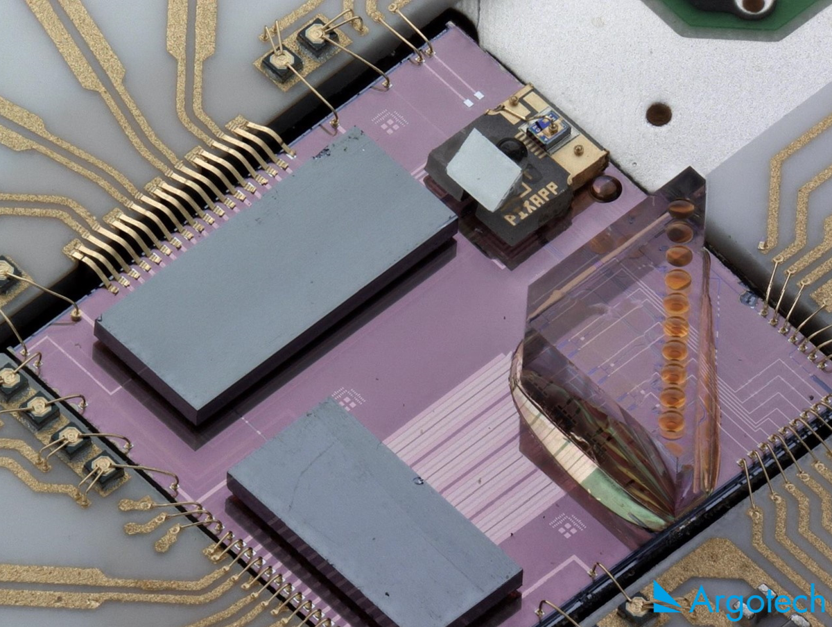
Silicon photonics chip and hybrid integration of CMOS IC, laser chips and optical block.
Połącz się z naszymi fachowcami: