How to prepare the data so that it does not get stuck during the production process
What to be careful of?
- Data must be complete.
This is a rule that is obviously known to everyone. But still minor flaws keep showing up. These might be files named incorrectly, without defined layers „.top“ and „.bot“ – witches of key importance for a correct and accurate assembly of the board.
- Do not export unnecessary layers.
The second typical mistake is exporting obsolete layers. Weed and get data that is not cleared of various auxiliary layers. Then that makes it extremely difficult for us defined and select the correct data amongst the cluster of the layers.
- Define the outline layer.
In case the layer is not complete and compact, and you define where the outline starts or where it ends only with crosses, for example, this might be another complication for us. As this is for the determination and specification of a sales offer so it is for the department of technical decorations. The software is used to having a compact layer.
Simultaneously it is crucial not to put the outline layer into all the layers as than it is hard in certain phases to remove it from various layers.
- Just a drillmap is not enough.
Please do not forget about the “drilling data”. The drillmap itself is just not enough. We might be able to turn it into a final draft but it is unnecessarily difficult and time consuming.
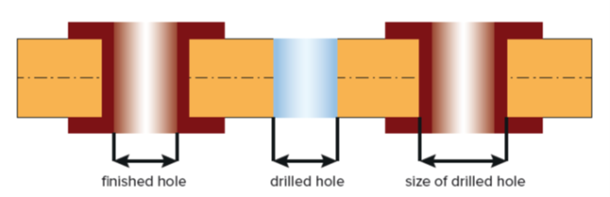
- A drilled vent and a final vent, these two are not identical.
With output data it is always highly relevant to consider with what vent diameters the circuitboard has been designed.
For instance in the case of vents there is a big difference between a final, result data and drilling data. Whereas with every board that is more than single layered the vent then is metalled and thus gets smaller. The technician in the preparation department needs a specific piece of information with what diameter the initial design is counting with. This is then reflected on the optimization of the data. If he does not have that specific piece of information or it is not clearly stated enough, the technician then takes entered diameters as final ones and he then increases the value in the data for production by approximately 0,10mm.
- What is supposed to be the final thickness of copper?
We also need clear information on the final thickness of copper. If our customer requires copper of thickness “18”, it is clear enough. But if we are to have specifications that, for example, I would like a “45” or a “70” copper, this piece of information does not clearly describe whether a basic copper or a final copper is being discussed. Basic copper is a fundamental core material and its thickness increases after metalling by a certain amount.
- Mark the layers
The ideal layer marking is described on our website, we are set on it.
We are, however, able to adapt to any kind of labeling, it is only important to export the layer labeling in the same way with every new order.
- Add your information file to the data.
If you have any other information regarding the circuit board stating what to be cautious about, what specifications it should have, it is always good to specify it not only in your order but also include this in the data.
- Consider the construction class.
Not every producer is capable of fulfilling just about any wish of their customers. Therefore we recommend making an effort to try to find out maximum amount of information from the website of the addressed producer. For instance in our company we normally process six construction classes-3 to 8. Momentarily, a ninth construction class is being tested in production. We successfully produce 0.15 mm vents with the halo of 75 microns. This covers vast majority of our orders and even in spite of this we do get a customer from time to time who we are just not able to serve.
- Count with the minimal width of the conductor and isolation gaps dependent on the used thickness Cu.
We have strictly set technical limitations upon layers that are metalled and on layers that are not metalled due to the used copper foil. Such technical specifications and limitations are stated on website at gatemapcb.com
If you keep these 10 points on your mind, chances for a correct and fast delivery of the board are increased fundamentally.
Połącz się z naszymi fachowcami: