Solder mask: everything you need to know
Application of permanent liquid solder mask
1. Application of photosensitive solder mask
The mask material is applied in the form of a viscous liquid or film to the entire PCB surface including future solder pads. After partial drying (curing), the photosensitive mask material is illuminated through the film, developed and finally cured. The film master is negative and covers the soldering and contact areas to be left unmasked. The non-illuminated, and therefore uncured, areas are washed away during development, thus removing the mask. Developing is followed by a final cure, usually thermal.
The more laborious process with a photosensitive mask allows for a much more precise and subtle pattern than direct screen printing.
2. Application of a solder mask by silkscreen printing
The application of a two-component solder mask by screen printing and its heat curing is technologically older. This mask is used less and only on single-sided plates. It is applied using a conventional silkscreen printing technique and after printing the resulting pattern is cured by heat or UV. As this is a conventional screen printing process, there is no need to deal with workplace lighting, but extraction must be provided.
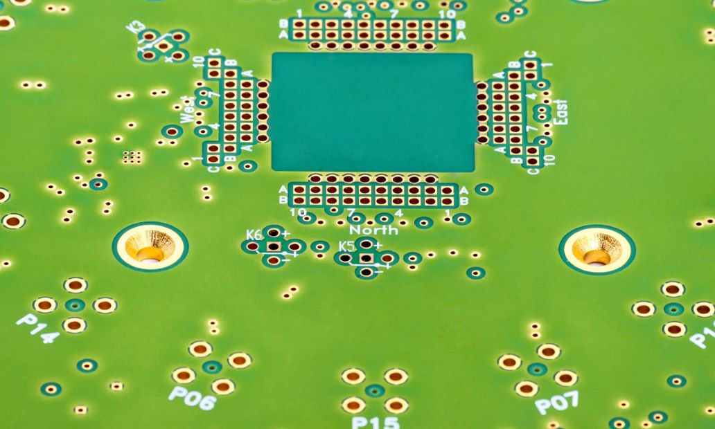
What is the purpose of the solder mask?
A solder mask is a durable covering layer applied to the surface of a circuit board so that only the solder and contact surfaces are exposed. The mask performs the following functions on the PCB. It protects the board from corrosion, mechanical damage and prevents the covered areas from getting wet. It also improves the electrical properties of the PCB, isolating the electric current. The solder mask was developed primarily with the wave soldering process in mind to prevent bridge short circuits and also to reduce solder consumption. The solder mask must be resistant to the fluxes and cleaning agents used.
4 main types of solder mask
Solder masks are made of different materials and are applied using different methods. The method and selection of the solder mask depends on the subsequent PCB application.
The mask, as a protective coating, is applied to the copper traces of the PCB during production. Each layer of coating contains a polymer material that protects the quality and functionality of your device's circuitry. The most common solder mask option is the application of an epoxy coating that protects all wires and circuit boards.
The photosensitive mask application workstation must have adequate lighting addressed, at a minimum by placing shielding films in the lamps.
Epoxy solder mask
This is the cheapest and most common type of solder mask available. Screen printing is required to print liquid epoxy on a printed circuit board. Screen printing has a woven mesh to block the ink. Epoxy liquid is a thermoset polymer that cures with heat. The dye mixed with the epoxy resin produces the desired colour.
LPI solder mask
Liquid photo-imageable solder mask or LPI (=Liqud Photo Imageable) is a more advanced type of solder mask, similar to those used by semiconductor manufacturers for photoresist exposure. Manufacturing operators can screen print the LPI or spray it onto the surface of a circuit board for a less expensive method of application.The etched and cleaned printed circuit is applied in an even layer in liquid form, exposed to UV light over films, and after developing and washing, the mask is cured. The epoxy resin is applied to the unmasked areas through a screen printing stencil with the pattern created. The final finishing process involves light UV exposure and thermal curing of the plate.
For more precise applications, operators use a more sophisticated method. They use photolithography technology to specify pad holes, mounting holes and solder mask holes.
Screen printing
- Screen printing is a stencil printing technique that allows the reproduction of single and multi-colour printed circuit boards using screen printing. The principle of screen printing is very simple - it is actually the extrusion of a viscous polymer substance through the permeable surfaces of a screen printing stencil. The stencil is usually a very thin fabric, nowadays usually plastic or steel. The actual shape of the print is created mechanically (by adhering a cover layer with a cut-out print motif or plotter) photochemically (by copying into a light-sensitive layer) or digitally (by evaporating the cover layer with a digitally modulated laser beam; CTS method). The thickness of the solder mask shall be 20 µm on average on the front surfaces and at least 10 µm on the edges of the pins.
Spray coating
- The printed circuit boards are conveyed by conveyor under a nozzle system that sprays the coating (solder mask).
Spraying through a shielded slot for the solder mask
- The conveyor moves the boards through the screen created by the paint (solder mask) flowing out of the slot.
Permanent solder masks DFSM (=Dry Film Solder Mask)
- Application by rolling
Similar to the LPI solder mask, it is necessary to expose the dry film solder mask. The PCBs are extruded between the heated rollers of a vacuum laminator. The rollers roll the photosensitive film unwound from the stock coil onto both sides of the plate simultaneously. The vacuum is designed to prevent the formation of air bubbles. After exposure, operators use a solvent to remove unexposed areas of the solder mask and cure the exposed film by applying heat.
Removable soldering mask
Is an elastic protective layer applied over the surfaces to be protected from soldering on tin wool. It is easily mechanically removed from the board after soldering. It can only be applied to PCBs with a HAL finish. The maximum diameter of the protected hole is 1.5 mm, the edge of the protected area must be at least 1 mm from the edge of the board, the distance between the protected area and the adjacent soldering area must be at least 0.4 mm.
The removable mask cannot be applied bilaterally over a single hole and cannot be used to protect unpunched holes.
For piece orders and in cases where a removable mask cannot be used, kapton tape is used as a full alternative to the removable mask.
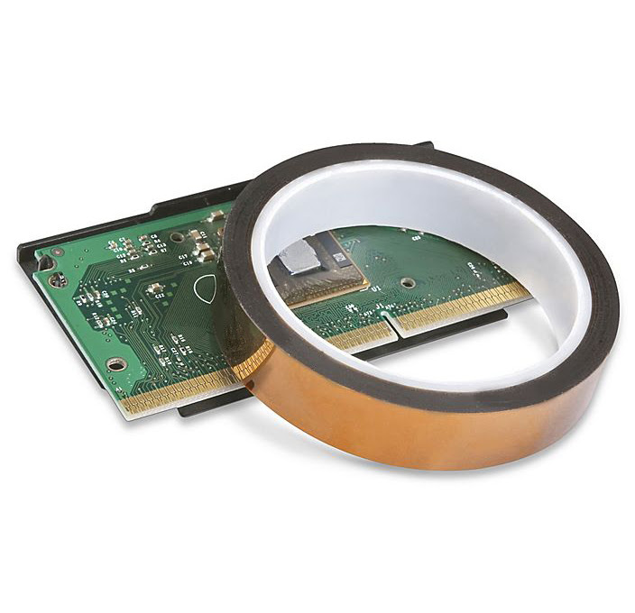
What is Kapton tape?
Kapton is a fully polyplastic, chemically polyimide. These are resistant to solvents, oils, acids and other chemicals. Kapton also does not degrade ultraviolet or alpha, beta and gamma radiation. Kapton tape is highly stable at low and high temperatures – it can withstand 180°C in the long term and up to 260°C in the short term. It is therefore more than suitable for protecting electronic board contacts during wave soldering and other high temperature applications in electronics.
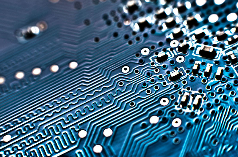
Colours of soldering masks
Initially, most circuit boards were green in colour. But now it is possible to get different colours of circuit boards. If the circuit board is completely or partially stripped when integrated with the final product, it is possible to obtain a circuit board with a color that complements the colour of the final product. In some cases, the top side will be one colour and the bottom side will be another colour. The green colour is not a solder mask per se, but is actually an oil colour.
However, different colours are available for solder masks, such as green, blue, black and white. The type of colour depends on the different applications. It is not a standard, but designers can use colour differentiation according to the application of the board.
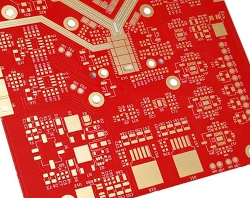
For example, on prototypes in the introduction phase of new products, they usually use a red solder mask. A different circuit board separates production and serial products. Solder masks are often chosen if the circuit boards are to be partially or fully visible to better match the final product. The white solder mask is again applicable to PCB for LED fixtures, it used to struggle with yellowing due to temperature and time, today there are materials that resist these properties.
Green colour
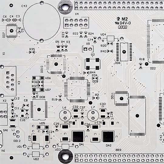
Green is still the most popular colour for solder masks. The main reason for this is that all inspection and overall work is easier with green PCBs. Research has shown that green does not tire the human eye as much and reflects copper surfaces, traces and voids.
Green is a solid choice when it comes to masking in a product. It also cures properly in processing, holds components well and exhibits the highest print resolution.
Red colour
Red masks are the preferred choice of many designers in the AI and IoT space. This may be because red creates a stronger contrast than other colors. It may also be because red sparks creativity and is simply more aesthetically pleasing.
Blue colour
There are many similarities between blue and green solder masks. However, more designers choose blue because it is more unusual in the market. Blue PCBs can serve just as a differentiator from existing production for prototype products.
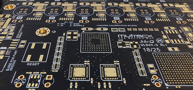
Black colour
Black masks do not attract as much attention, even though they have a longer life and better protect circuits that need to maintain durability. Because black absorbs heat more than other colours, there is no risk of the solder melting during soldering. At the same time, black paint is less noticeable in black electrical equipment.
White colour
White masks are rarely used because they provide less visibility of grommets and connections. White solder plates turn yellow after a while, especially when exposed to high temperatures. On the other hand, they are ideal for LED systems because they are brighter than any other color.
Solder masks in the design
In general, you need to cover the entire PCB with a solder mask, except for component mounting areas and perhaps points you plan to use as test points. The overlap of the solder mask into the solder pad is 0.04 mm. If it were not there, there would be a risk of damage to the PCB. And if you want to know all the technical information related to the design rules for solder masks, then have a look.
Połącz się z naszymi fachowcami: